Electronics production
Back when creating circuits using breadboards, the boards can be too big to conceal in our artifacts, hence in this topic we learn how to create our own PCB boards.
Back when creating circuits using breadboards, the boards can be too big to conceal in our artifacts, hence in this topic we learn how to create our own PCB boards.
Our method of manufacturing PCB boards will be using a FR1 PCB.
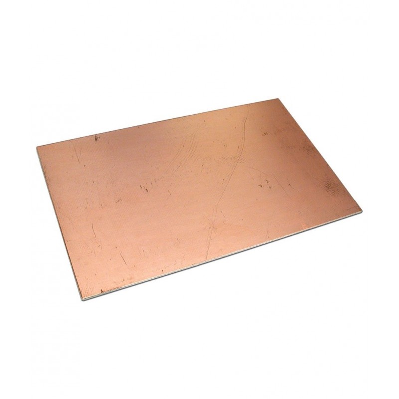
It basically has a thin layer of copper on Phenolic paper, where we will use a CNC machine to cut out the board and remove the copper layer to form the connections before soldering the electronics on.

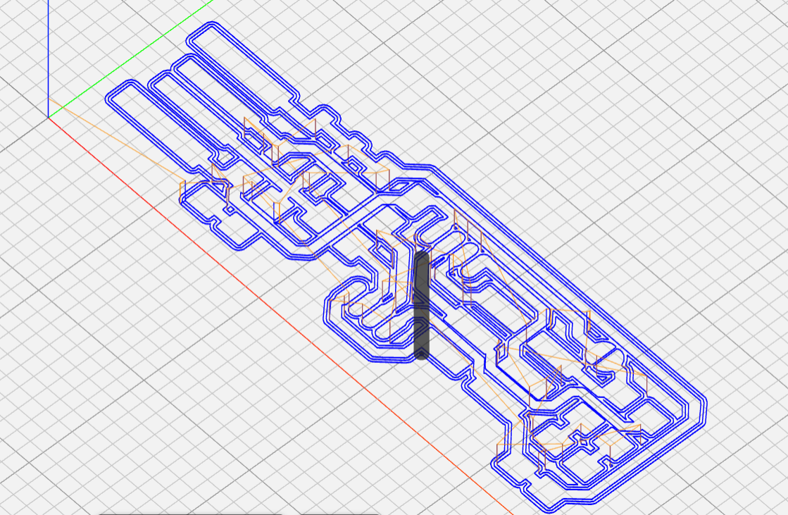
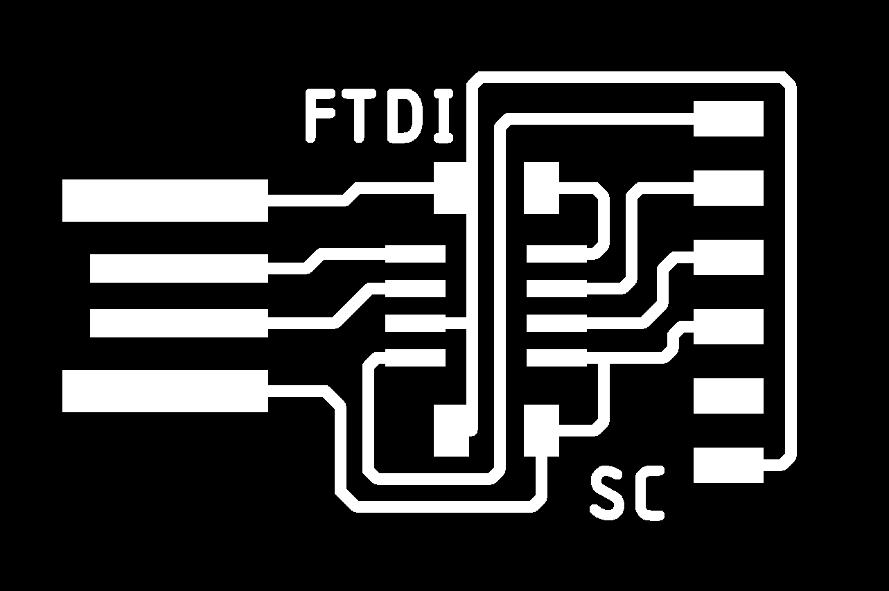
First we learn how to manufacture an FTDI board from a png file schematic.
We will need the board outline cutout and the traces.
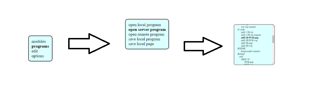
After downloading the images we need to convert the images to g-code in order to give instructions to the CNC machine to cut. For this we used mods.
At the website, right click then select programs > Open server program, under G-Code select "Mill 2D PCB png".
I next insert the png file name and set the configurations. The only parameters I will need to change is Mill traces 1/64 under "Set PCB Defaults", tool diameter, cut depth, max depth and offest under "mill raster 2D" and cut and plunge speed under "path to G-code".
.png)
I then click calculate. A separate page will open, showing the results. The G-code file is auto downloaded.
.png)
I then insert the outline image, reconfigured the values and saved the G-code.
.png)
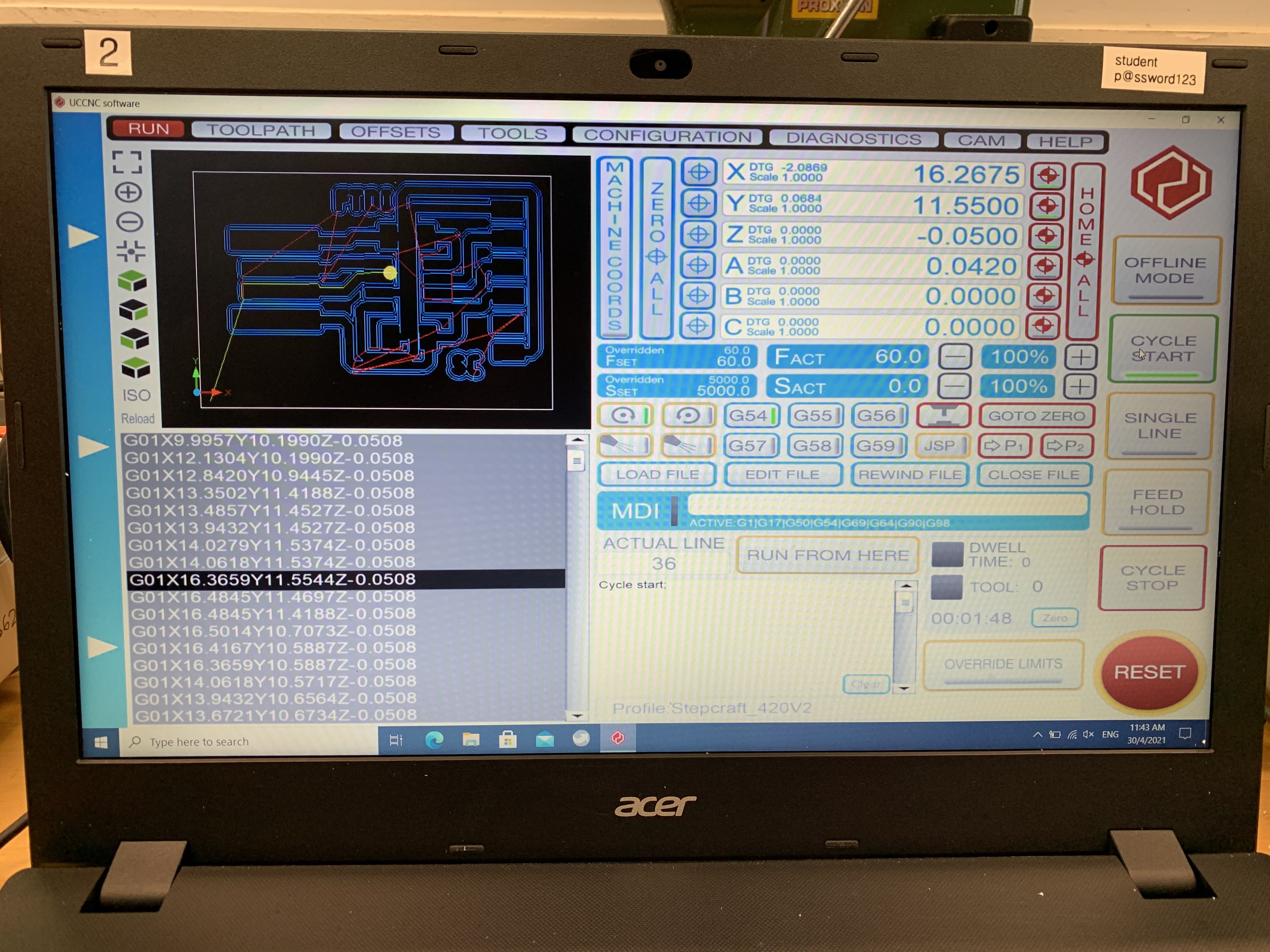
To evaluate the G-code, you can upload the file on ncviewer.com.
.png)
.png)
Once the G-code is done, we can use it on the Stepcraft CNC cutter to fabricate the board.
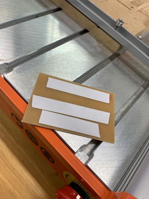
Secure the board with double sided tape and stick it to the work surface. Ensure the tape does not fold or overlap as it can cause the board to not be level and affect the cutting process. Also ensure the work surface is clean.
For the traces, I used a 0.1 mm 30 degree V-bit, while for the board outline I used a 0.8 mm flat endmill.
Once fitting the toolbit onto the drill I set the Z-axis using the provided probe.
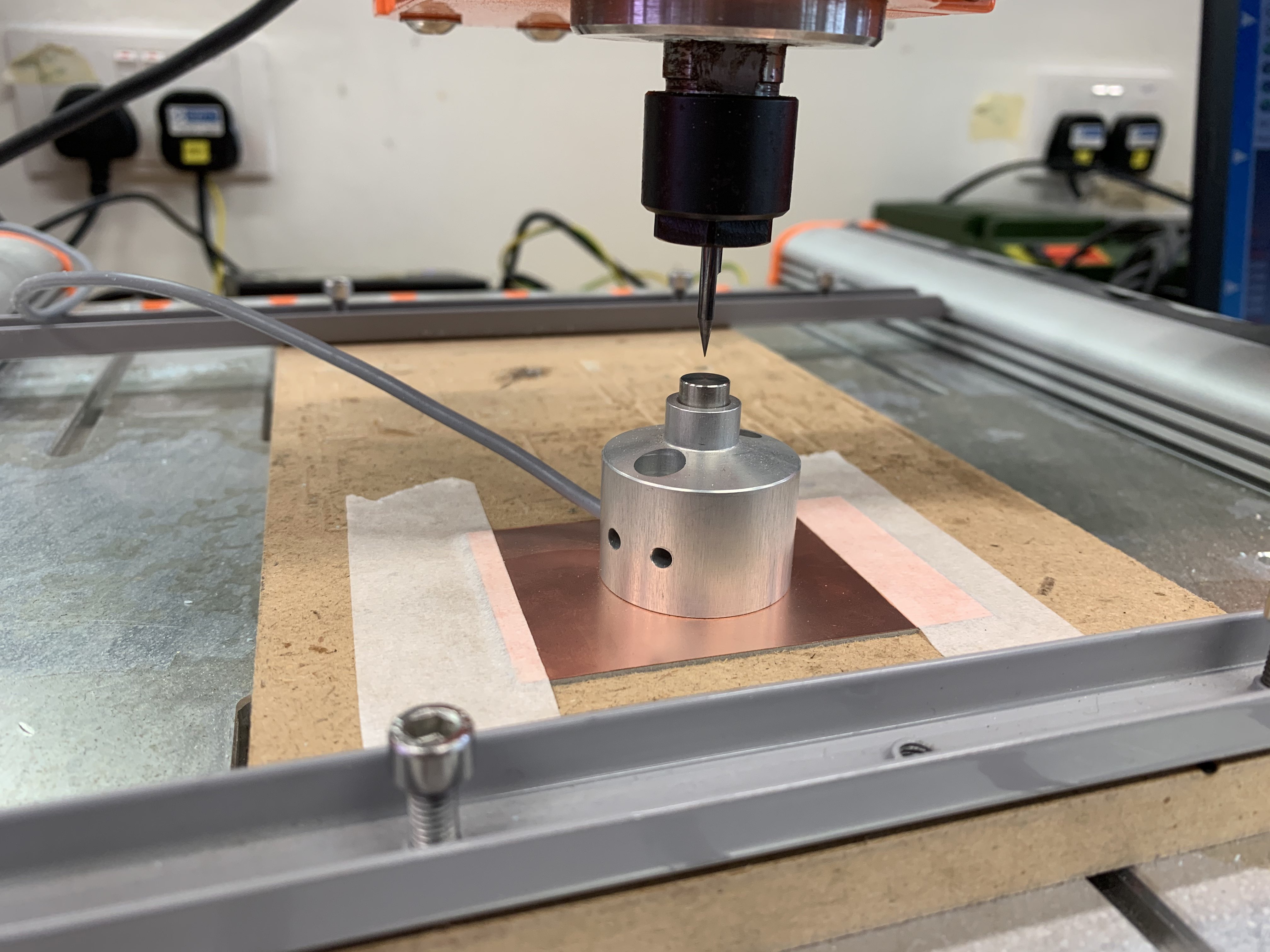
I first upload the traces code and set the X and Y to the edge of the board. Then the board is ready to cut.
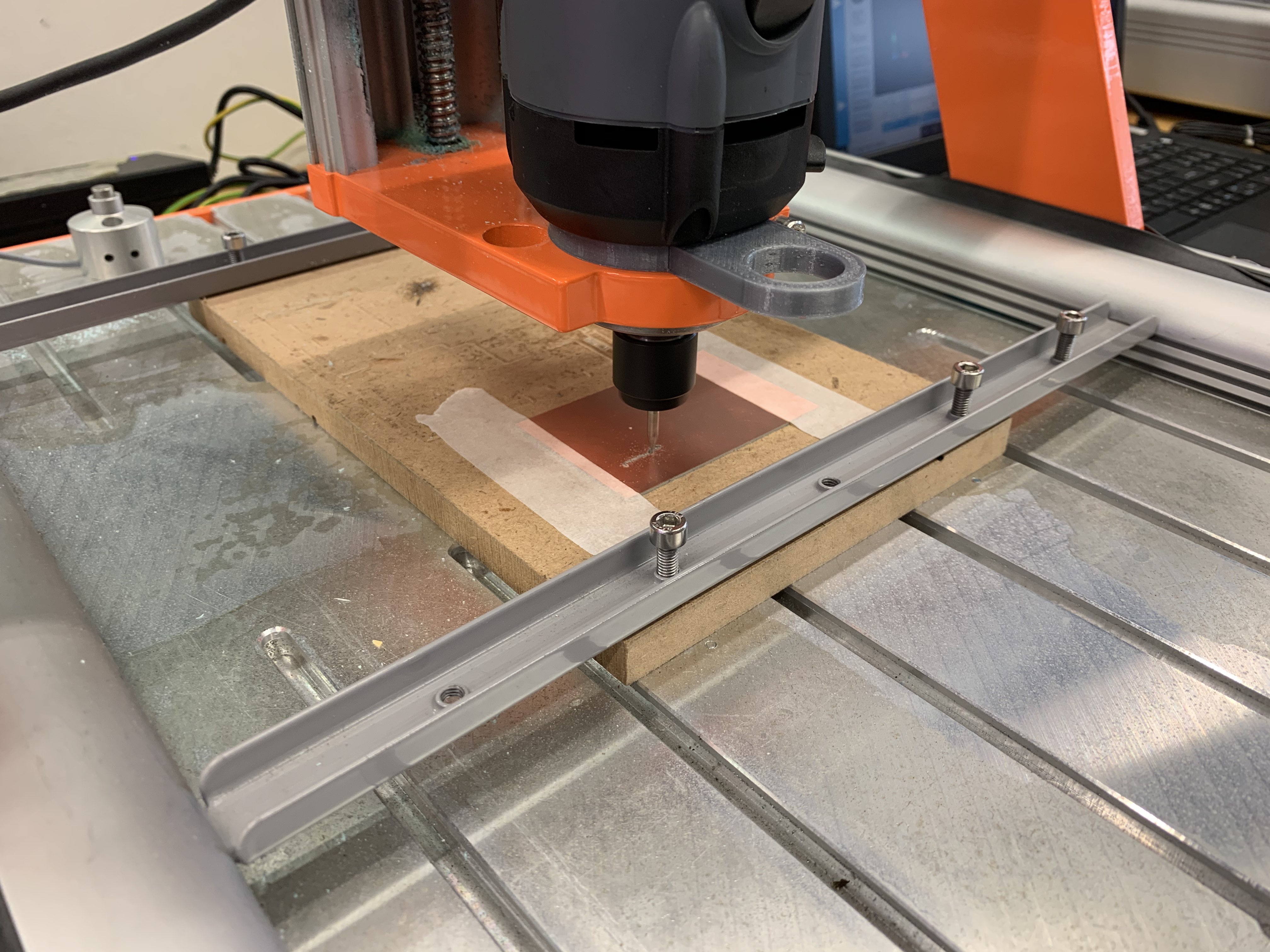
After the traces are done I switched the tool bit, recalibrated the Z axis and uploaded the outline code.
As the end board cuts were rough I used a sandpaper to sand it down, and here is the end product:
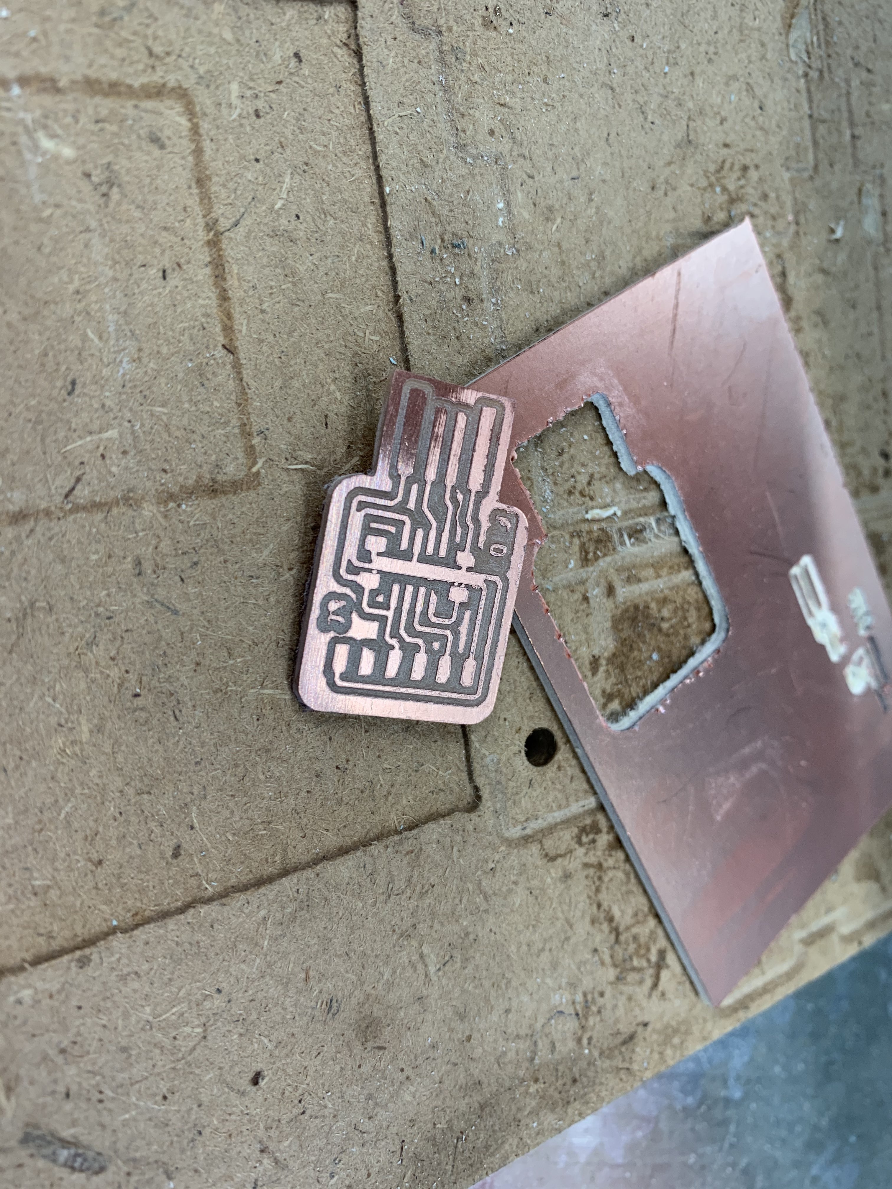
After this you can design your own PCB and fabricate it out, here is an ATTINY85 echo board.
